Inner-layer copper reliability of electroless copper processes
October 08, 2015
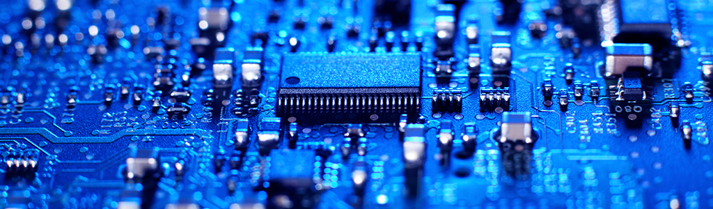
Today’s printed circuit boards (PCBs) continue to evolve, driven by changes in laminate materials, routing density and assembly techniques. At the core of these PCBs is the metallization process, required to make the drilled holes conductive, creating the interconnections that will give the finished board its functionality. Electroless copper (Cu) plating technology from Dow Electronic Solutions is an essential part of many of the world’s leading PCB high-volume manufacturing lines. One of the critical challenges of this technology is achieving interconnect reliability. This article looks at some of the common issues related to PCBs and the importance of understanding material interactions to achieve manufacturing control.
An electroless Cu process is designed to make the dielectric laminate material that is exposed during the via formation process (mechanical or laser drill) conductive, so that subsequent electroplating processes are able to plate the holes to the required Cu thickness, normally ~25 microns. The electroless Cu process must be engineered to provide coverage of the dielectric material while also ensuring that the inner-layer interconnects are able to meet reliability requirements.

Figure 1: Poor Cu adhesion creates interconnect defects (ICDs), adversely impacting interconnect reliability.
Interconnect reliability is essential to overall PCB performance, and understanding the materials, mechanical and chemical processes used to manufacture these circuit boards—is needed to ensure the best possible reliability. Since the board materials used have higher coefficients of thermal expansion (CTE) than copper, when the PCB is exposed to elevated temperatures during the assembly process, the dielectric expansion leads to an increase in the stress at the inner-layer interconnections. Therefore, good adhesion between the copper plated in the through-hole and the inner-layer copper is essential to reliable PCB function; otherwise, poor adhesion can lead to ICDs, as seen in Figure 1.
ICDs may be detected using quality control (QC) checks of coupons from working panels after the plating process, normally after circuit formation. The most common method used is thermal stress, also called solder float testing, and may consist of multiple solder floats at 288°C, or higher, depending on materials, etc. Following the thermal stress testing, microsections are prepared and evaluated by optical microscope for presence of failures. Also, protocols for both thermal stress and thermal cycling (e.g., IST or HATS testing) have been established to quantify ICD performance, so that experiments using different materials and process conditions can be evaluated.

Figure 2: Example of an interconnect after thermal stress with no defects as observed by optical microscope.

Figure 3: ICD Type I separation occurring at the inner-layer copper/electroless copper interface, often related to poor controls within the electroless Cu process

Figure 4: ICD Type II separation occurring at the electroless Cu/electrolytic Cu interface for various reasons: post-electroless-Cu cleaning residues, contaminated pretreatment prior to electrolytic plating, or an out-of-control electrolytic Cu process.

Figure 5: ICD Type III separation occurring within the electroless Cu layer itself, typically due to poor controls within the electroless Cu process
Both methods of forming vias—mechanically drilled through holes, or laser-drilled micro-vias— generate significant localized heat and resin-containing debris that appear as “smear” on the inner-layer or capture-pad Cu surfaces. If this smear is not completely removed before the electroless Cu, it forms a barrier between the Cu surface and the subsequently plated Cu, and may result in an ICD. Smear may be removed by a wet chemical de-smear process, or a plasma etching process. In both cases, it is important to evaluate the effectiveness of the de-smear process for each type of laminate material used.
In recent years, both inorganic and organic fillers have been added to high-speed, high-Tg laminate materials to improve physical and electrical properties. However, as filler is increased, the machinability of the laminate changes, normally requiring evaluation of drilling and de-smear processes to ensure their effectiveness. Unremoved filler material may become embedded in the copper surfaces of inner layers, which may lead to ICDs. The most commonly used fillers can be detected by the presence of elements including silicon, aluminum and calcium; ICDs of this type may be identified by using techniques such as EDS or XPS to analyze the elemental composition of the defect area.
Interconnect reliability is essential to overall board performance. To ensure the best possible reliability, it is critical to understand the relationships between the laminate, the mechanical and chemical process parameters, and controls. Our team works with customers to solve these challenges, using our expertise in PCB manufacturing, plating processes and our deep understanding of how to fine-tune chemical formulations to be able to provide complex functionalities.
Related Information
DuPont’s metallization & imaging products are key enabling technologies for high-end multi-layer boards used in computers, smartphones & automobiles.
We’re here to help.
We love to talk about how our electronics solutions can build business, commercialize products,
and solve the challenges of our time.