Semiconductor Fabrication and Packaging Materials
End-to-end materials solutions to support the semiconductor manufacturing process
DuPont’s rich history of experience and innovation has deep roots in the semiconductor fabrication industry. Our broad portfolio and expertise support many segments, from advanced chip manufacturing processes, to advanced packaging and assembly, to compound semiconductor device fabrication.
We offer complementary, reliable, high-quality materials sets to support both today’s high-volume manufacturing processes and advanced technology for the future. Through close collaboration with our customers, we develop solutions to address leading-edge technology challenges that are critical to advancing diverse market drivers. We work with our customers to develop or place materials that meet their specific needs, including technical performance and cost-of-ownership improvements.
Our materials are valuable building blocks for today’s advanced microelectronics found in everything from consumer electronics to high-end data centers, automotive applications, medical devices, the Internet of Things, artificial intelligence, power electronics and more.
-
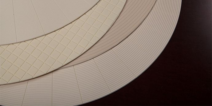
What are Semiconductor Fabrication Materials?
At DuPont, we define semiconductor fabrication materials as chemistries and other products critical for wafer processing in the fabrication of silicon die, including microlithography, chemical mechanical planarization, and cleaning solutions, through to advanced wafer-level packaging processes, as well as other related technologies.
Semiconductor Materials
-
Materials for Chemical Mechanical Planarization (CMP)
Materials for Chemical Mechanical Planarization (CMP)
CMP pads and slurries tailored to each customer's needs
A range of offerings for chemical mechanical planarization (CMP) including Novaplane™, Optiplane™, Acuplane™ and Klebosol® slurries. -
Lithography Materials and Services
Lithography Materials and Services
Learn how DuPont develops and delivers market-leading lithography materials to support semiconductor advanced patterning.
DuPont’s robust, production-proven photoresist product line offers materials options that meet the requirements across generations of lithography processes.Anti-reflective coatings and sublayers boost the effectiveness of lithography by widening and improving the process and reflectivity windows.Used in conjunction with photoresists, DuPont’s advanced overcoat materials are designed to prevent defects and improve the lithography process window, enabling finer feature patterns.DuPont’s roots run deep in its production-proven line of ancillary lithography products. From developers, removers, and other enhancement chemistries, we support a total lithography solution.DUV and 193nm photoresist performance begins with the polymer, and DuPont electronic grade polymers continue to improve upon existing techniques for polymer manufacture, isolation, and evaluation. -
Specialized Removers and Clean Chemistries
Specialized Removers and Clean Chemistries
Specialty removal and clean chemistries for use in post-chemical mechanical polishing (CMP) and post-etch processes.
Learn about our post-CMP copper interconnect cleaner required in the manufacturing of advanced semiconductor devices.Aqueous & semi-aqueous organic mixtures formulated to effectively remove residues from substrate surfaces after via, poly and metal etch processes.Enable removal of positive- and negative-tone photoresists as well as plasma-hardened residues, and which are compatible with a wide variety of metals required to form LED contacts.Formulations optimized to effectively remove thick and thin resists used for TSV masks and wafer bumping by solder electroplating or stencil printing.EKC4000 PCT is a cost-effective replacement that outperforms conventional "rinse" chemistries such as IPA and NMP. It quickly and effectively eliminates corrosion on the wafer surface caused by drag-out (carry over) of chemistry from prior wet cleaning. EKC4000 PCT is compatible with automatic equipment and is formulated to meet ULSI grade specifications for advanced wafer treatment. -
Dual Damascene Copper
Dual Damascene Copper
Since 2006, leading-edge semiconductor manufacturers have relied upon DuPont Electronics & Industrial's dual damascene products for achieving semiconductor technology nodes below 20nm. What's our secret?
-
Semiconductor Packaging Materials
Semiconductor Packaging Materials
With more than 50 years invested in technology development, DuPont Electronics & Industrial understands the needs in the market and has developed a broad portfolio of semiconductor packaging materials for a range of technology areas.
DuPont offers positive- and negative-tone photoresists designed to meet the tight pitches and varied topographies of today’s semiconductor advanced packaging applications.Our production-proven Copper pillar formulations work in perfect harmony with our under-bump metallization (UBM) and tin-silver capping chemistries, to provide a seamless solution for all your Copper pillar needs.DuPont Electronics & Industrial copper chemistries for redistribution layers (RDLs) are ideally suited to today’s high-density requirements for wafer level packaging applications.Look to DuPont for packaging dielectric formulations that have the mechanical properties, high resolution, low-temp curing, easy processes, and superior reliability needed to protect your advanced WLP.DuPont’s award-winning Solderon™ BP electroplating chemistries are a reliable alternative to tin-lead alloys for all wafer bumping applications.Years of experience and success in electroplating damascene copper have helped DuPont bring leading-edge copper TSV chemistries to the advanced packaging market.We offer a production-proven electroplating nickel chemistry tailored to meet a variety of UBM process needs. -
Semiconductor Assembly Materials
Semiconductor Assembly Materials
By working in collaboration with leading-edge packaging and assembly houses, DuPont Electronics & Industrial sets the bar for excellence. Our materials are developed based on the latest requirements and are proven in high-volume manufacturing.
Ordinary die-attach adhesives suit ordinary chip applications. But when a chip design must deliver reliable performance in extreme temperatures, high moisture, or stressful environments look to DuPont Electronics & Industrial for extraordinary solutions.Our silicone die encapsulants maintain reliable performance even at the high reflow temperatures required for lead-free solder processing or stringent thermal stress-reliability testing conditions.DuPont’s portfolio of silicone-based lid-seal adhesives are designed to handle the high functionality of today’s advanced packaging processes, delivering the performance needed for today’s high-performance computing, mobile and automotive electronic applications.Photo-patternable dielectrics and non-photo-patternable adhesives make possible chip-to-wafer and wafer-to-wafer stacking for heterogeneous integration.Our thermally conductive silicones are designed to handle the heat dissipation of today’s advanced electronic devices. -
Silicon Precursors
Silicon precursors are high-purity gas or liquid materials used in key steps during the manufacture of semiconductor devices.
We’re here to help.
We love to talk about how our electronics solutions can build business, commercialize products,
and solve the challenges of our time.