Fan-out wafer-level packaging materials evolution
July 06, 2016
Recently, fan-out wafer level packaging (FOWLP) has become one of the hottest advanced packaging technologies in the market. Although it made its first appearance in 2009 with the introduction of embedded wafer level ball grid array (eWLB) from Infineon, it wasn’t until recent market requirements for miniaturized system in package (SiP) solutions in mobile applications brought FOWLP to the forefront. Essentially, FOWLP fills the performance gap between organic laminate SiPs that are limited to 10µm line and space, and Si interposer solutions that are more costly, but offer <1µm l/s.
In part one of this two-part series, we examine the back-story of FOWLP and the markets it serves. Part 2 will discuss managing mechanical properties of FOWLP.
FOWLP provides electrical connections with physical protection to silicon semiconductor integrated circuit (IC) chips, allowing circuit traces to be reliably routed for connection outside the die. FOWLP takes pre-diced known-good silicon chips and reconstitutes them using a mold compound into either a round wafer or a rectangular panel for further processing. Using a wafer or panel-level processing, the copper (Cu) bumps/pillars, redistribution layers (RDLs) and solder bumping are added for off-chip connections.
FOWLP evolved from fan-in WLP (FIWLP also known as WLCSP), which in turn evolved from flip-chip (FC) packaging.
- Flip chip was introduced in 1968 by IBM using the “controlled collapse chip connection” (C4) technology; it uses solder balls in a peripheral or area array to make connections from the package to the substrate.
- FIWLP starts with a dense peripheral array of contact pads at the edge of the chip, then adds a redistribution layer (RDL) to route traces to a less-dense area-array configuration. Since the I/Os are limited to the surface of the die, this package is limited to low-end devices requiring up to 200-300 I/Os.
Advanced ICs are now so filled with circuitry that the number of needed connections exceeds the area on the chip for area-array formation, therefore mold material is used to expand the available area around the chip for additional RDL routing in FOWLP.
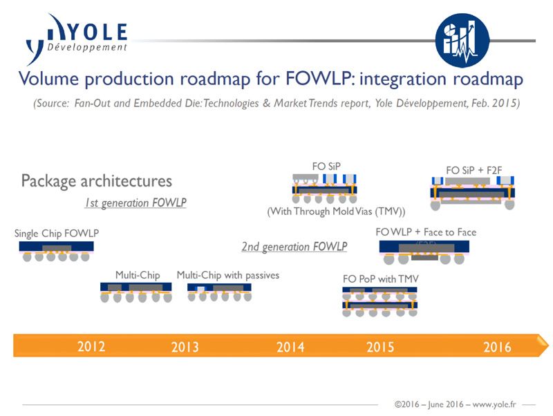
Figure 2: The evolution of FOWLP (Source: Yole Développement)
Figure 2 shows simplified cross sections of FOWLP and how it has evolved over time to meet the increasing integration needs of high-volume manufacturing (HVM) of ICs. The first generation of FOWLP includes a single flipped chip (shown in gray) surrounded by mold material (shown in black)to expand the area for routing out to solder balls. The 2nd-generation of FOWLP technology is for multichip packaging (MCP) in general, and allows for heterogeneous integration of different chip types such as logic, memory, analog and RF communications. FOWLP allows for vertical integration of various devices and packages, to form completely functional systems-in-package (SiP).
Much of the need for FOWLP comes from the requirements for small, ultra-thin packages and fast circuit speed, primarily driven by the wireless and mobile markets. Mobile devices require chips in packages that provide maximum performance and power efficiency with small physical size.
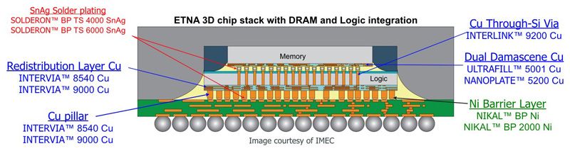
Figure 3: Cross section of a 3D chip stack with DRAM and logic integration
Figure 3 shows the use of through silicon vias (TSVs) to allow an FC memory chip to have the shortest and therefore fastest connections to a logic chip inside a single package. TSVs provide maximum IC performance, but require redesign of the logic chip to allow for placement, and call for complex testing procedures, such that use of TSV is expensive and delays product release.
Chips destined for cloud computing applications may have sufficiently high profit margins and long life cycles such that IC designers can afford to use TSVs, while mobile chips have inherently short product life cycles and are cost sensitive that generally preclude such use. One of the main advantages of FOWLP is its ability to vertically stack dies without the need to redesign the chips. In addition, it enables thinner and lower cost packages, therefore, it is the advanced packaging segment expected to have the highest growth in the coming years

Figure 4: Revenue forecast by advanced packaging platform shows strong growth for FOWLP from 2014-2020 (Source: Yole Développement)
Assembling multiple chips in multiple layers requires more electrical connections, which in turn requires both thinner lines within the RDL and an increase in the number of RDL layers. The RDL line width of 1st-generation FOWLP started in the 10-15µm range, but has already been shrunk to 5µm in HVM. Outsourced assembly and test (OSAT) companies are now working in R&D to develop 2µm wide line/space (L/S) capability and smaller to meet the requirements of today’s high-end applications. The most advanced FOWLP designs in R&D today use up to eight layers of RDL for multichip routing. The ability to reliably achieve such integration is significantly impacted by the performance and characteristics of the materials and processes applied.
Part two of this series will examine some of the specific material requirements needed to address the challenges in FOWLP designs.
Related Information

DuPont's Rob Kavanagh talks about the impact FOWLP adoption has on advanced packaging materials.
We’re here to help.
We love to talk about how our electronics solutions can build business, commercialize products,
and solve the challenges of our time.