Copper electroplating fundamentals
Lucy Wei
Global Segment Director, Circuit Metallization, Interconnect Solutions
November 22, 2016
Copper Electroplating Bath
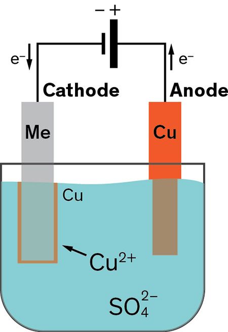
The concept of copper electroplating is straightforward: Submerge the wafer to be plated into an electrolyte bath, apply a current, and copper ions will migrate and deposit onto regions with a pre-existing metal seed layer.

Figure 1: Image of electrolytic plating cell
The electrolyte bath contains three primary inorganic components:
- Copper sulfate (CuSO4) provides a source of copper ions.
- Sulfuric acid (H2SO4) makes the bath conductive and acts as a charge carrier.
- Chloride ions (Cl-) combine with the organic species to form a complex that slows down plating rate on selective areas.
For advanced packaging applications, it is important to carefully control the copper plating rate and deposition location. Several organic plating bath additives help achieve the desired results:
- Accelerators form electroactive species responsible for enhanced plating rate.
- Suppressors combine with chloride ions to inhibit plating on areas where a reduced plating rate is desired, and can also act as a wetting agent.
- Levelers polarize the areas with high current densities and even out current distribution, and help control the surface morphology. Organic additives may act somewhat differently depending on the electroplating application.
Copper Electroplating Applications
|
|
Dual Damascene |
TSV |
Cu Pillar |
|---|---|---|---|
|
Feature size (example) |
20 nm X 170nm |
10 x 100 µm |
20 x 20 µm |
|
Bottom Up Fill Time |
A few seconds, (<= 1 sec. for 1X nodes) |
~40 min. |
~7.5 min. |
|
Accelerator |
High concentration |
Medium or low |
Medium or low |
|
Suppressors |
Strong polarizing agent, Fast wetting |
Wetting and polarizing agent |
Wetting and polarizing agent |
|
Levelers |
Polarizing agent for field (top of trench) |
Polarizing sidewall of via |
Polarizing in the via |
Figure 2: Chart of Cu electroplating in semiconductor packaging applications
Semiconductor packaging uses copper electroplating in several important applications: dual damascene process, through-silicon vias (TSV), copper pillars, and copper redistribution layers (RDL). In each case, feature geometry as well as plating time affect how additives behave.
Dual Damascene Plating

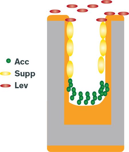
Figure 3: Illustration of dual damascene copper plating
The dual damascene process is used for very small features, in the range of tens to hundreds of nanometers, which are filled in a few seconds or less. This requires a high concentration of accelerator molecules at the bottom of the trench or via. The suppressor adsorbs to the side wall and serves to inhibit side-wall deposition, enabling bottom-up filling. The leveler typically remains at the top surface and slows over-plating to give a smooth deposit for easy chemical mechanical planarization (CMP).
Through-silicon Via Plating

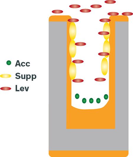
Figure 4: Illustration of copper TSV plating
TSVs are relatively large and have a higher aspect ratio than found in DD. Filling vias that are 10 µm wide and 100 µm deep takes less than 60 minutes. The accelerator reaches the bottom of the via, while the suppressor and leveler both adsorb on the side walls and wafer surface, where they minimize the risk of voids forming and lower the overburden Cu during the long plating process.
Copper Pillar Plating

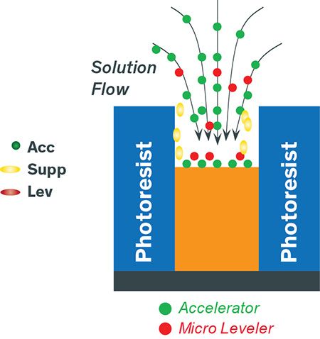
Figure 5: Illustration of Cu pillar plating
Copper pillars are constructed with a different fabrication method. Unlike TSV and DD wafers, which are coated with a copper seed layer across the entire wafer, pillar wafers have a copper seed layer only at the bottom and photoresist that has been patterned on top to define the features. Suppressor wets the photoresist and the leveler enters the via during the 7- to 8-minute plating process, to help create a pillar with a flat top. Both leveler and suppressor are polarizing agents that help control the plating uniformity across different die and wafer. The accelerator acts as a Cu grain-refiner, making a smooth and bright deposit.
Redistribution Layer Plating

Figure 6: Plated redistribution layer, 50 μm bond pad with 10 μm lines
Despite the very different shape of the final features, redistribution layer (RDL) patterns have similar structure as copper pillar patterns during electroplating (i.e., photoresist to define RDL dimension). The function of additives in RDL plating is similar to those in copper pillar plating.
Future tutorials will delve more deeply into challenges and solutions for TSV and copper pillar electroplating.
Related Information

Copper plating forms critical connections from horizontal RDLs through vertical pillars.

The key structures for FOWLP and considerations for managing material properties.
DuPont understands the market needs and has developed a broad portfolio of semiconductor packaging materials for a range of technology areas.
We’re here to help.
We love to talk about how our electronics solutions can build business, commercialize products,
and solve the challenges of our time.