Increasing smartphone functionality through novel metallization
Vincent Chen,
Application Technology Engineer
February 05, 2019
When was the last time you used your smartphone to simply to make phone calls? More often than not, we use them for anything but what they were originally designed to do. Rather, our smartphones have become a complete communications hub and personal assistant from which we read email, conduct business, search the web, text our friends, post our social status, capture memories, log our steps and calories, monitor our homes, hail rides, shop, watch movies, listen to music, date, and more via a host of apps. Despite market saturation, or maybe because of it, high-end smartphone manufacturers continue to compete for market share by adding more input/output (I/O) on device circuitry to support all the increased functionality in smartphones needed to run these apps. Getting right down to the nuts and bolts of smartphone manufacturing, more I/Os means finer printed circuit board (PCB) Line/Space (L/S) requirements.
One way manufacturers have achieved finer L/S requirements is by trading in traditional PCBs for high-density interconnection (HDI) PCBs. The current L/S capability used in mass-produced smartphones using HDI PCBs is 35/35µm L/S. However, driven by the Apple iPhone 8 and X, L/S requirements are targeting 30/30µm, according to a recent report by Yole Development. To remain competitive, other high-end smartphone manufacturers like Samsung and Huawei are transitioning away from HDI PCBs to substrate-like PCBs (SLPs), which are essentially circuit boards that have package substrate features.
For HDI PCB manufacturers, the 30/30um L/S requirement cannot be achieved by traditional subtractive processes with high enough yields for volume manufacturing. Since a subtractive process is not a good solution for 30/30um L/S, the industry is starting to look at additive processes. While there are many different additive processes, one quick answer for fine line solutions is the semi-additive process (SAP), which has been used by package substrate PCB manufacturers for many years. Technically, SAP has the capability to reach as low as 10/10um even 8/8um L/S, so it can easily achieve 30/30um L/S.
However, if SAP is chosen as the solution for 30/30um L/S, then HDI PCB manufacturers would need to: (1) invest a lot of new equipment, specially designed for SAP, which is very costly; (2) run different process with different materials, for example, a new dielectric, Ajinomoto Buildup Film (ABF), which would have a longer learning curve for manufacturing and result in a higher technical entry barrier. So, given the major cost and technical challenges, SAP is still far away from adoption by today’s HDI PCB manufacturers for a 30/30um L/S solution.
So, if SAP isn’t a compelling solution, is there a fine line process that needs less equipment investment and has fewer technical barriers? In fact, a Modified Semi-Additive Process (MSAP) has been developed to lower the technical entry barrier and to reduce the cost for HDI PCB manufacturers. As shown in Figure 1, SAP starts with a dielectric (e.g. ABF), while MSAP starts with copper clad laminate (CCL), either a thin Cu CCL or using a Cu reduction process, technologies which are much more familiar to HDI PCB manufacturers. Although both SAP and MSAP contain Desmear/electroless Cu, SAP needs a much better combination between the Desmear and electroless Cu so that it can provide the adhesion required for electroless Cu to stay on the dielectric. Once again, this is a totally novel process to HDI PCB manufacturing. By contrast, MSAP starts with CCL and other familiar process used in today’s HDI PCBs, so from a cost and manufacturing learning curve point of view, it provides a good solution for PCB manufacturers to move from HDI PCB to SLP.
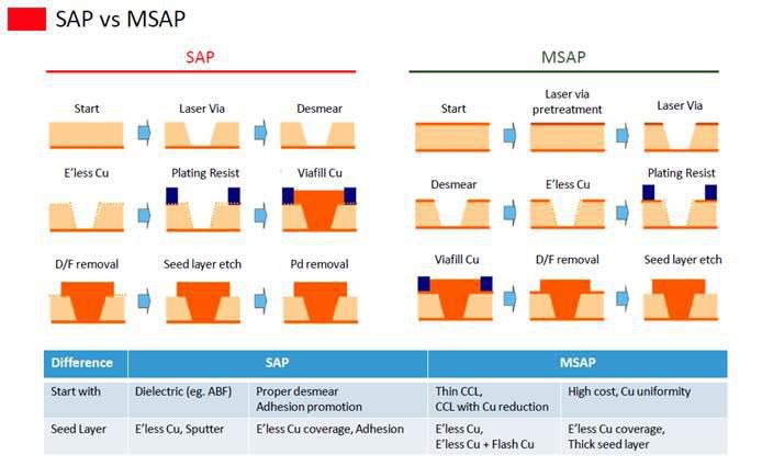
Figure 1: Comparison of conventional SAP and MSAP metallization process flows.
Because SAP is used for package substrate PCBs, PCBs run using MSAP are called “Substrate-Like PCBs” (SLP). Currently, the technology used in the iPhone8 and X starts with a 3µm base, and then adds 0.4µm of electroless Cu plus 5µm of flash Cu followed by 18-22µm of Cu via fill, resulting in a total Cu thickness of 28µm. To achieve a final Cu thickness of 20µm requires a complicated etch process to remove the extra 8µm. Some refer to this SLP as a first generation SLP.
The current process still has some disadvantages. Because it plates extra Cu and then etches it back, it not only increases the possibility of technical and reliability issues, but also increases the cost of manufacturing. Therefore, several approaches have been developed to improve this for second generation SLP. One idea, called advanced modified SAP (amSAP), eliminates the flash Cu and uses thick electroless Cu plating to create a 1.6µm layer followed by 18-22µm of Cu fill. This still requires an etch step to remove 5µm of Cu to achieve a total thickness of 20µm. Alternatively, DuPont’s electroless Cu plus flash Cu (ELF-process) combines electroless Cu plating with flash Cu plating in a single step, adding 0.1 and 0.9µm Cu, followed by 16-18µm of Cu fill. The total Cu is ~20µm, with no etching back required. This simple process eliminates the reliability concerns that accompany thick electroless Cu plating. Already qualified for use in high-end flexible PCB (FPCB) manufacturing processes, the ELF process is suitable for next-generation MSAP on SLP (Figure 2).

Figure 2: ELF, a novel metallization process for MSAP, delivers uniform Cu metallization at 1.0µm thickness, eliminating the need for costly and complicated etch back processes.
Conclusion
DuPont’s ELF process combines electroless Cu plating with flash Cu plating to reap the benefits of both in a single step. ELF makes it possible to form a 1µm conductive Cu layer quickly, to meet ever the shrinking L/S requirements for SLP production. Also qualified for FPCB applications, the ELF process is a novel metallization solution that enables increased functionality in high-end smartphones.
Related Information
The growing size and complexity of the automotive PCB market makes it a great opportunity for PCB suppliers.
We’re here to help.
We love to talk about how our electronics solutions can build business, commercialize products,
and solve the challenges of our time.