Copper pillar electroplating tutorial
Lucy Wei
Global Segment Director, Circuit Metallization, Interconnect Solutions
December 08, 2016
In a previous tutorial, we provided an overview of copper electroplating for advanced packaging applications, including both via filling and copper pillars. The requirements and processing considerations for electroplated copper pillars for flip chip applications are somewhat different than those for via filling, and warrant additional discussion.
Evolution of Bumping
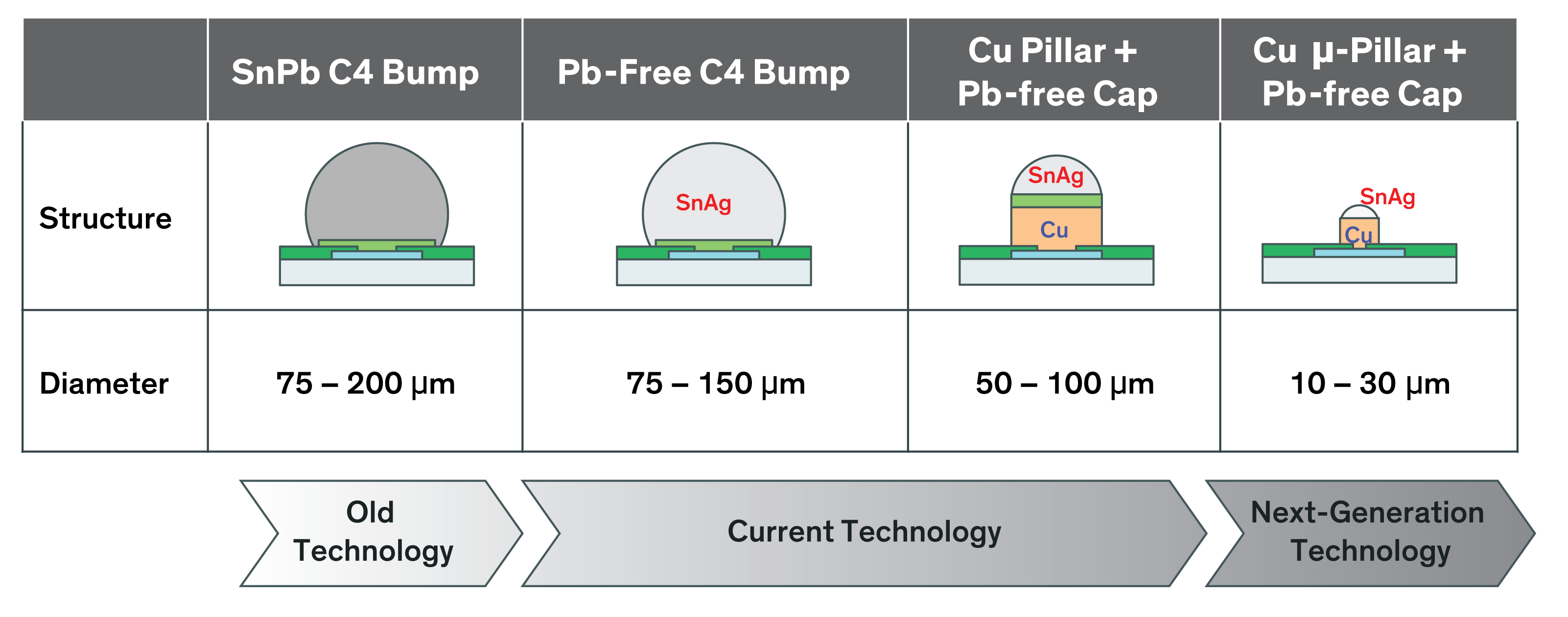
Figure 1: Bumping technology generations
Copper pillars are now common in flip chip interconnection, usually with a lead-free SnAg solder cap on top. The transition to copper pillars has been driven by the limitations related to size and pitch (space between features) of traditional controlled collapse chip connection (C4) bumping. As pitch requirements continue to shrink, copper pillars can enable higher-density designs while maintaining sufficient bump height. The next-generation technology will feature pillars as narrow as 10 to 30 µm.
Copper Pillar Plating Process
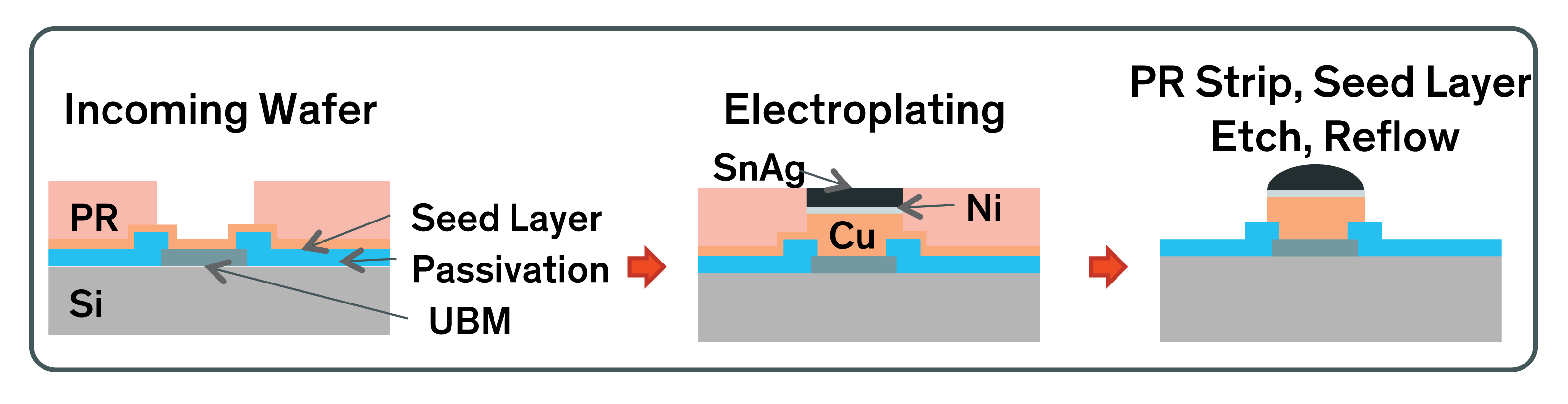
Figure 2: Illustration of the tin-silver capped copper pillar plating process
Copper pillars are electroplated over a Cu seed layer at the base, with photoresist defining the diameter of the pillar. A nickel diffusion barrier between the pillar and the solder cap limits formation of a copper-tin intermetallic layer at the interface or prevents formation of microvoids. Excessive intermetallic growth and microvoids can both negatively affect reliability. When used with copper chemistry that has exceptionally high purity, this nickel barrier may or may not be needed, depending on customer preferences.
Design and Performance
|
Design Goal |
RDL Target |
20 μm Pillar Target |
RDL Target |
50 μm Pillar Target |
|---|---|---|---|---|
|
%WID Uniformity |
<5% |
<5% |
<5% |
<5% |
|
Plating current desties |
2 to 12 ASD |
4.5 to 12 ASD |
4.5 to 18 ASD |
20 to 40 ASD |
|
Total Doping |
<20 ppm |
<20 ppm |
<20 ppm |
<20 ppm |
|
Solder Compatibility |
Void-free w/o Ni Barrier |
Void-free w/o Ni Barrier |
Void-free w/o Ni Barrier |
Void-free w/o Ni Barrier |
|
|
|
|
|
|
Figure 3: Typical design goals and performance targets for copper pillars
Proper choice of electroplating materials and processes ensures that pillars meet certain design goals, chosen to optimize quality and reliability. Keeping the impurity level in the plating bath as low as possible minimizes the risk of developing voids at the pillar-solder interface. If dopants such as carbon, sulfur, chlorine and other impurities are kept below 20 ppm, it is possible to form a void-free capped pillar even without using a nickel barrier layer.
Effects of Electrochemical Potential
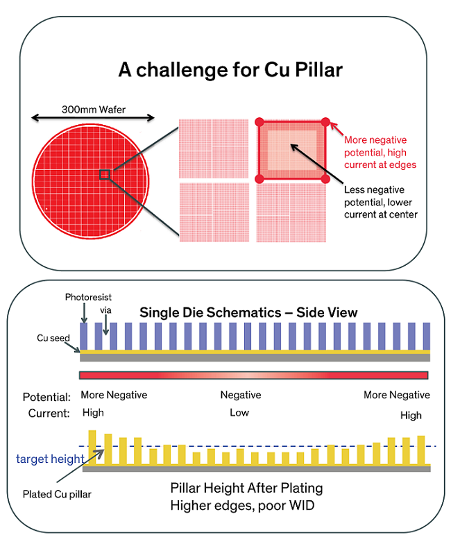
Figure 4: Within-die uniformity
Pillar height needs to be consistent for proper die attach, but electrochemical potential is not uniform across each die on a wafer. It will be higher at the edges and corners, resulting in taller bumps at the edge and therefore insufficient contact at the center of the die, where the pillars are lower. The higher the bump density, the greater the challenge.
Understanding Within-die Uniformity
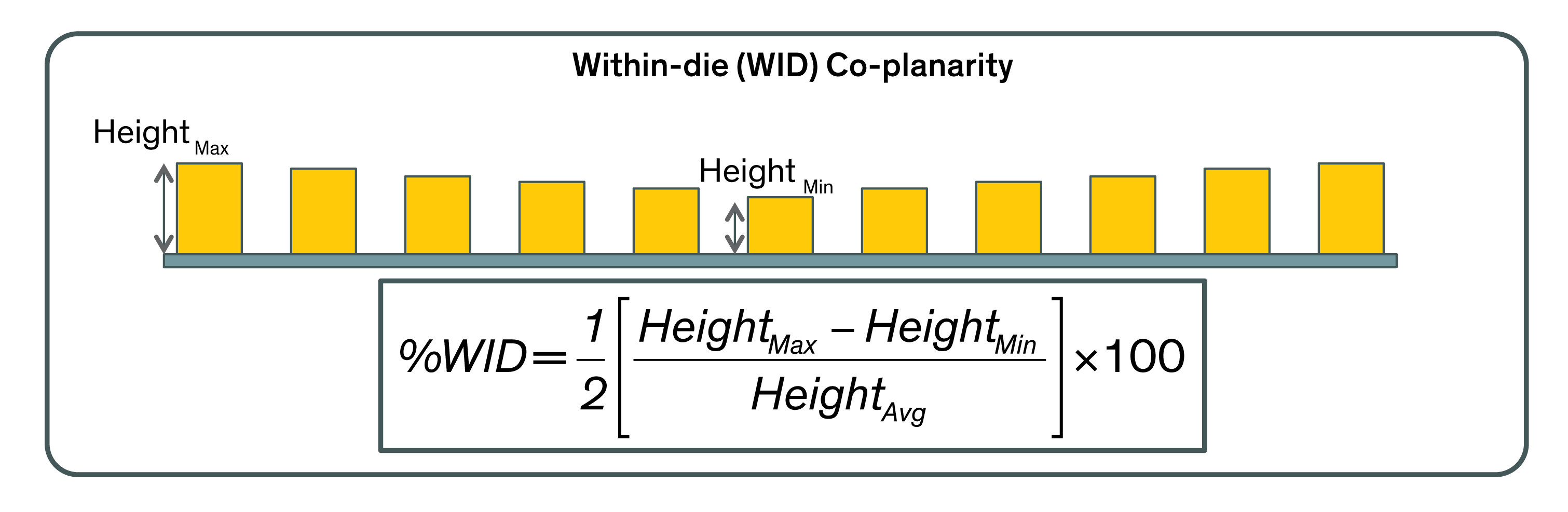
Figure 5: Calculating within-die uniformity
Within-die (WID) co-planarity or uniformity, calculated as shown in figure 5, should usually be less than 5%, although the target may be higher for larger pillars. A lack of WID uniformity within these parameters will cause reliability issues.
WID Control through Chemistry
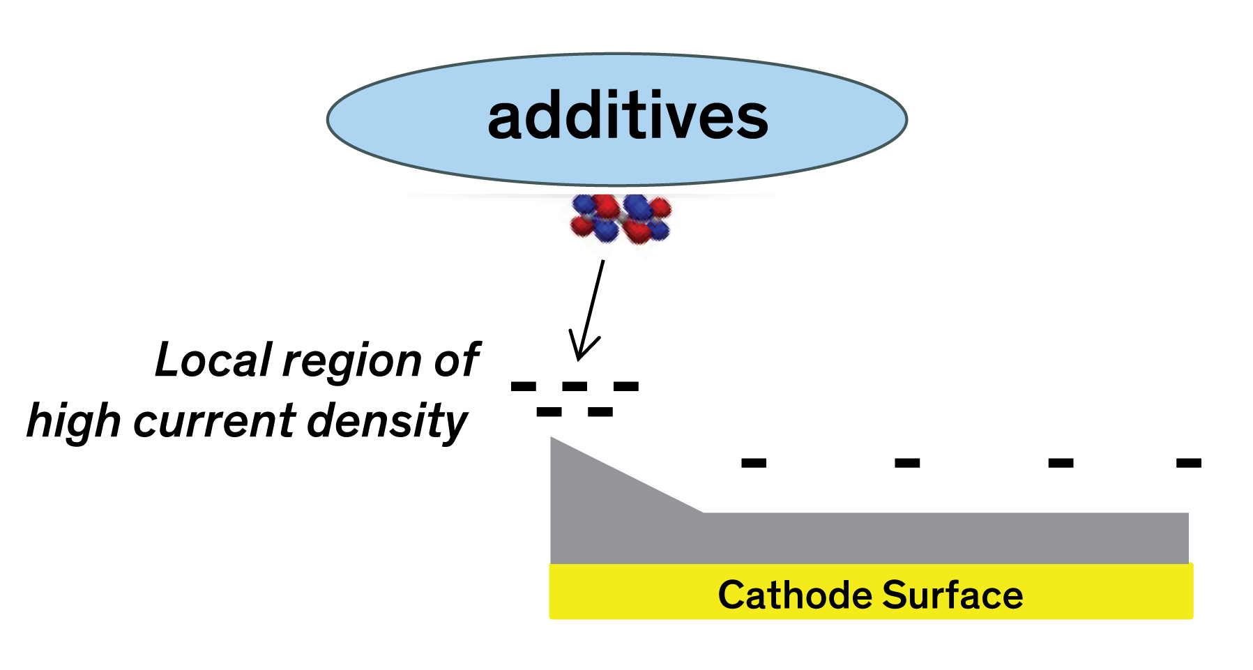
Figure 6: Role of additives in controlling within-die uniformity
Optimized additives in the electroplating bath can help achieve appropriate WID uniformity. Levelers are preferentially attracted to regions of higher current density, where they suppress electroplating rate and create a more uniform array of pillars.
Calculating Dome Shape
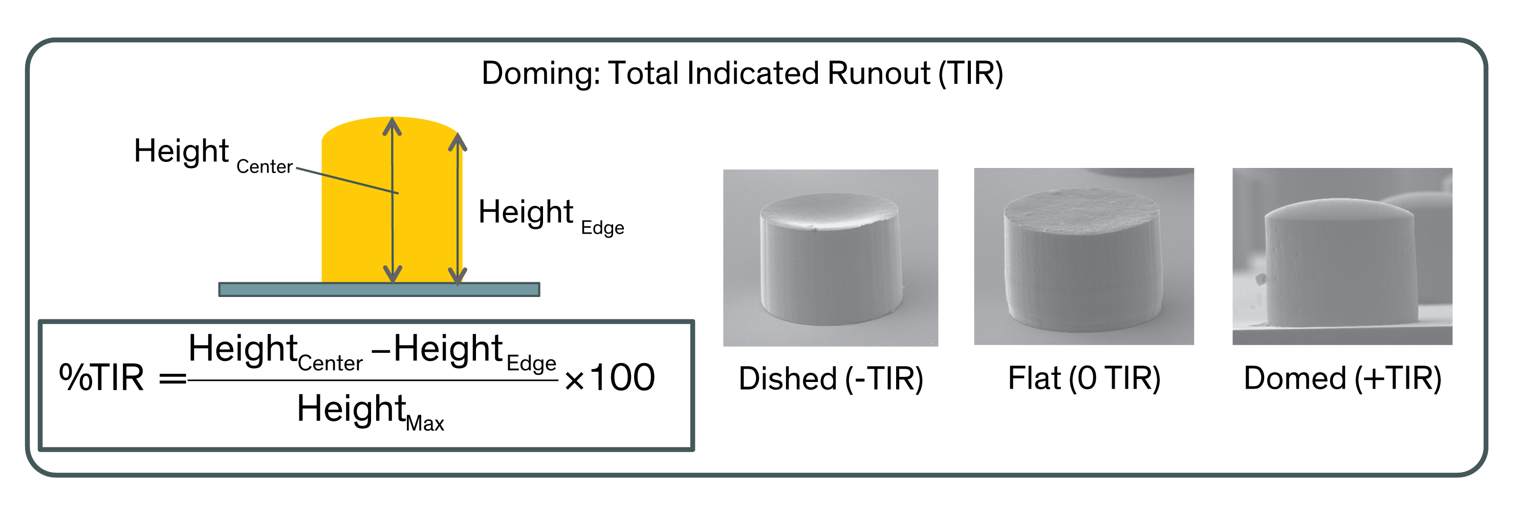
Figure 7: TIR calculation and examples of copper pillar shapes
Achieving a uniform pillar shape that will be optimum for subsequent solder plating and consistent across a die presents an engineering challenge. Most customers will prefer flat pillars, though occasionally a slightly domed shape may be helpful. The best electroplating materials and processes allow engineers to tailor the profile for each application. In any case, total indicated runout (TIR) should be kept within a range of ± 5%.
Balancing Pillar Shape and Voiding
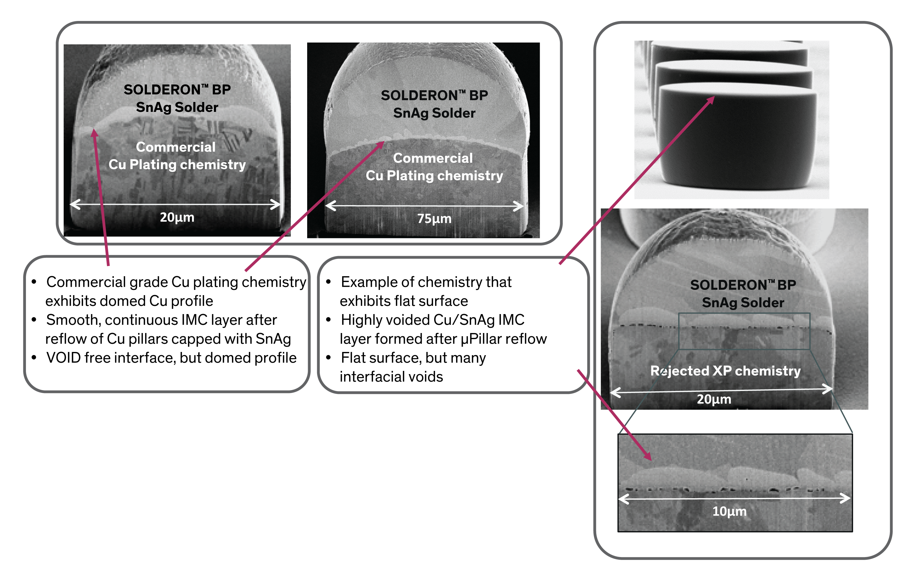
Figure 8: Shown are domed tin-silver capped copper pillars with void-free intermetallic compound (left) and flat copper pillars exhibiting extensive voiding between the copper and tin-silver interface(right)
It is not difficult to achieve flat pillars with the use of additives, but unfortunately, this sometimes comes with a poor pillar-solder interface, also commonly known as intermetallic compound (IMC), that contains multiple voids. Many commercially-available plating baths that produce high-quality interfaces often create pillars that are excessively domed.
Successful Integration of Flat Cu Pillars with SnAg Capping
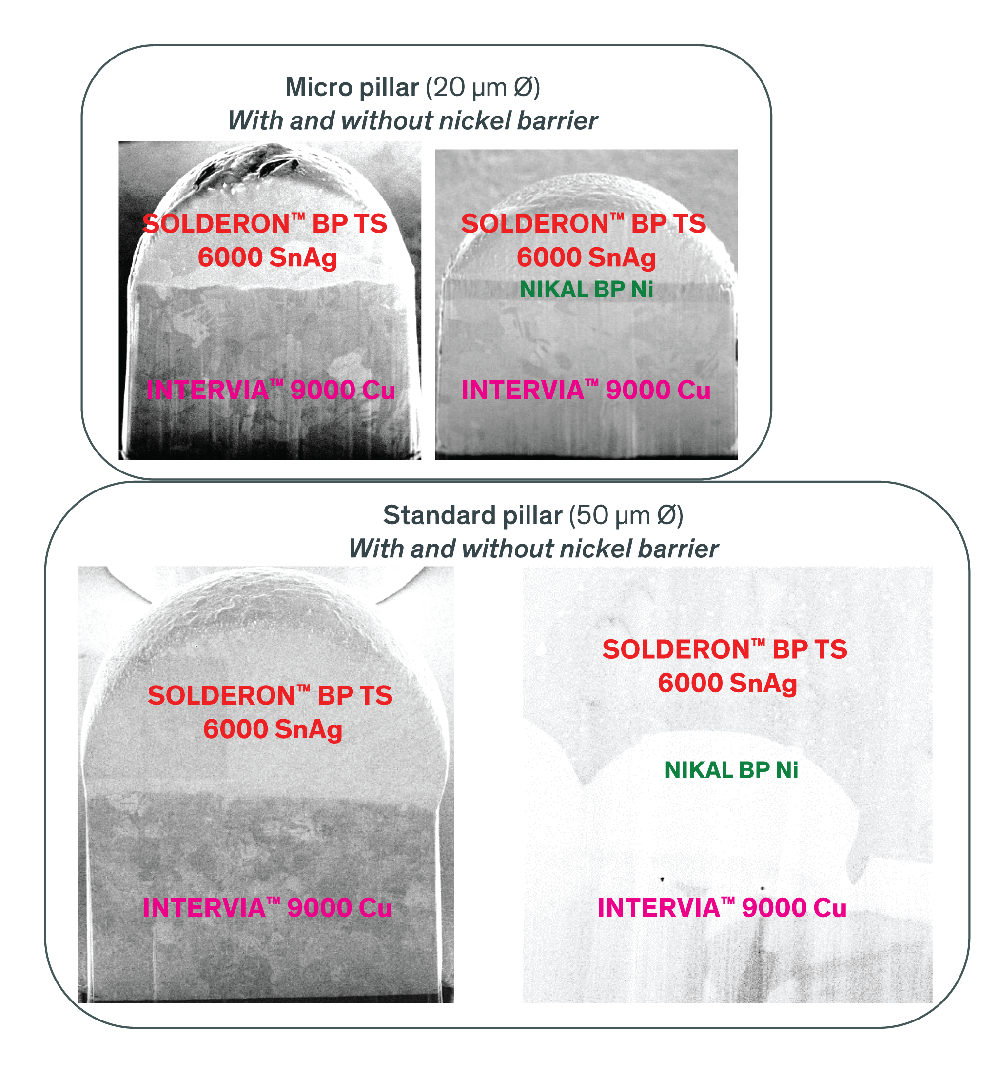
Figure 9: Void-free capped micro and standard copper pillars with and without Ni
Plating baths with optimized additives and copper purity can enable the best of both worlds: a flat pillar with a smooth, continuous interface, with or without a nickel barrier.
Related Information

This tutorial examines the concept of copper electroplating and how the process works, as well as its use in advanced packaging applications.

Copper plating forms critical connections from horizontal RDLs through vertical pillars.
DuPont is a market leader in high-performance, high-reliability metallization for printed circuit boards.
We’re here to help.
We love to talk about how our electronics solutions can build business, commercialize products,
and solve the challenges of our time.