Examining unique TSV plating challenges
Lucy Wei
Global Segment Director, Circuit Metallization, Interconnect Solutions
January 17, 2017
In a previous tutorial, we provided an overview of copper electroplating for advanced packaging applications. Through silicon vias (TSVs) present some unique plating challenges due to the long process time and high aspect ratio, and it is worth discussing these in more detail.
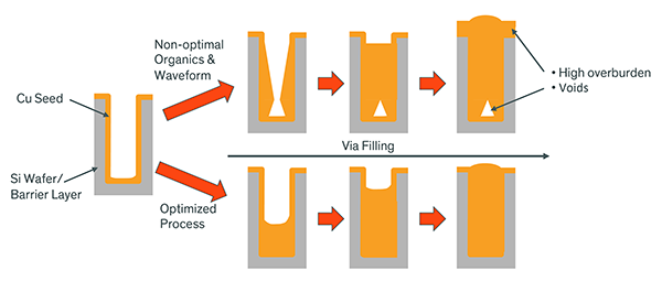
Figure 1: Illustration of non-optimal via filling process (top) and optimized via filling process (bottom) for TSV electroplating
Engineers in charge of designing fabrication processes for wafers with TSVs are aware that TSV filling is one of the longest steps in the fabrication process. It is natural to want to increase current density to achieve higher throughput, but faster, uncontrolled filling often leads to decreased reliability and increased chemical- mechanical planarization (CMP) cost.
Examples of Poor TSV Plating

Figure 2: Example of poor plating in TSVs with center seam voids
High current density can affect conformal plating, leading to center seam voids. The faster the fill speed, the more likely the formation of such voids, as well as excess copper at the top of the via (overburden).

Figure 3: Examples of poor plating in TSVs with bottom voids (left) and pinch off voids (right)
Uncontrolled or incomplete plating of TSVs will also result from poor selection of additives or improper concentration of additives in the plating bath. Poor wetting of vias can cause bottom voids (left), which can also result from bad seed layer coverage. Lack of polarization at the top of the via can cause pinch off voids (right) because the plating rate on the sides and top isn’t adequately slowed relative to the plating rate at the bottom of the via. (See Copper Electroplating Fundamentals tutorial.)

Figure 4: Examples of proper bottom-up via filling (test vehicle source: Applied Materials)
Proper selection of additives is important to create an optimum, void-free fill at high current density. The right materials enable fast filling–for example, 20 minutes for 5x50 µm vias and under an hour for 10x100 µm vias–with reliable fill from the bottom of the via up. Strong polarization at the via opening is essential to ideal filling profile.

Figure 5: Examples of low overburden during TSV plating (test vehicle source: Applied Materials)
Optimally-filled vias exhibit a very low overburden, which decreases the time required for subsequent CMP before depositing the next layer of material. Reduced CMP time translates to reduced costs for materials and processing.
The Importance of Bath Stability

Figure 6: Illustration of unstable vs. stable via filling processes
Bath stability presents another challenge to TSV electroplating. Quality may be excellent with a fresh bath, but as the organic additives break down, they can create undesirable byproducts that can result in voids in the vias.

Figure 7: Example of under-filled TSVs due to bath instability
Underfilled vias are often one of the first signs of bath instability. Additive breakdown leads to incomplete polarization, which can cause more copper to deposit in the field rather than entirely within the vias.

Figure 8: Example of how plating bath stability over time provides optimal TSV plating performance (courtesy of Applied Materials)
It is not trivial to achieve a stable process over thousands of wafers, but it is possible with an optimized electrolyte and additive package that is tailored to the plating tools. An optimized plating bath can remain stable for over 40 amp-hours per liter, enough to process 10,000 wafers with 5x50 µm vias or 4,000 wafers with 10x100 µm vias.
The Effects of Copper Purity
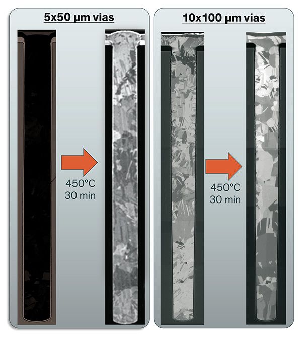
Figure 9: Examples of annealing high-purity copper in TSVs (courtesy of Applied Materials)
The level of impurities in electroplated copper affects its performance after annealing. Annealing should refine the copper grain structure without introducing voids, but excessive levels of impurities in the plating bath can cause problems. Studies show that electroplated copper with less than 25 ppm impurities maintains a void-free fill after annealing, which is not the case with a lower-purity material.
Creating reliable TSVs with high throughput can be a challenge, but with the right electroplating materials, the challenge can be overcome.
Related Information
Learn about Cu pillar requirements and processing considerations for advanced chip packaging.

This tutorial examines the concept of copper electroplating and how the process works, as well as its use in advanced packaging applications.

Copper plating forms critical connections from horizontal RDLs through vertical pillars.
We’re here to help.
We love to talk about how our electronics solutions can build business, commercialize products,
and solve the challenges of our time.