Fine-Line Patterning for SLPs Calls for High-Resolution Photoresist
Eric Lin and Kate Kao, DuPont Electronics & Imaging
August 12, 2019
The drive toward miniaturization recently inspired major smartphone manufacturers to tear some pages from the IC substrate manufacturing playbook and create a new generation of printed circuit boards (PCBs) known as substrate-like PCBs, or SLPs. The fine-line patterning used in SLPs provides a competitive advantage in the never-ending race to pack more function into a smaller smartphone footprint.
Why fine-line patterning is shrinking
While handset thickness and area remain relatively constant at 7-8 mm and 90-100 cm2, respectively, phones are expected to process more data without any noticeable lag. Doing so while maintaining battery life expectations requires a more powerful battery.
Meeting combined demands of long battery life, high performance, and size constraints calls for handset designs in which the battery takes up a greater fraction of the available space, shrinking the motherboard from around 25 cm2 to 15-20 cm2.
For the next generation of iPhones hitting the market in 2019 and 2020, the motherboard takes up less than 18 percent of the phone surface. At the same time, high-frequency signals must be transmitted at high speeds without loss. The answer is finer-pitch PCBs.
High-density interconnect (HDI) designs made with a 50-µm line width and spacing (L/S) have now migrated to 30/30 or 25/25 with the same number of layers, putting pressure on all the manufacturing process steps and requiring a shift away from standard subtractive PCB manufacturing toward semi-additive processes (SAPs) usually associated with HDI IC substrates.
Semi-additive processes create finer lines
Smartphone manufacturers discovered that modified SAPs (mSAPs) could be used to create fine-line patterning on SLPs used in their flagship phones. As SLP technology migrates into mainstream smartphones and other applications such as medical devices, automotive and aerospace, mSAP technology is poised for double-digit annual growth.
The growth in mSAPs poses both an opportunity and a challenge. By carefully selecting materials and equipment that maximize yield and reliability and implementing space-saving designs, manufacturers can best take advantage of the growing market.
The difference between SAP and mSAP
As its name implies, mSAP is slightly different from SAP, although both mSAP and SAP are used in making IC substrates. While SAP begins with a coating of electroless copper, mSAP begins with a laminated copper (Cu) foil. Both processes involve stacked, laser-drilled microvias to build up the layers. The additive part of the manufacturing process relies on depositing Cu on top of patterns defined by the photoresist rather than plating the entire surface with Cu, patterning, and etching.
The mSAP technology is still evolving, and future directions will include processes that are custom designed to accommodate the needs of fine-line PCBs
The advantages and demands of mSAP
While the window for mSAP begins around 60 µm L/S, subtractive processes are still an option for that relatively large pitch. Subtractive technology reaches its limits below an L/S of 30 µm, at which point mSAP must take over. Today’s mSAP processes in development target a value of 25 µm, with 20 µm on the horizon, making the technology attractive for applications needing denser PCB designs.
The mSAP process conveys advantages beyond finer-line resolution, however. It provides better electrical performance and the potential to save space, materials, and energy when compared with standard HDI processes. By replacing some subtractive processing steps that are inherently wasteful with additive steps that use materials more efficiently, manufacturers can achieve both a financial and an environmental benefit.
For PCB manufacturers accustomed to subtractive processes, the mSAP marks a significant shift. While it is possible to use materials and equipment designed for standard PCBs for many process steps, building reliable SLPs will be easier if facilities leverage mature technology from IC substrate manufacturing.
Because PCBs are much larger than substrates, however, and made from different materials, it isn’t possible to manufacture PCBs on a substrate fabrication line without modifying the process. As pitches shrink from 70 to 50 to 30 µm, hybrids of PCB and IC substrate manufacturing are likely to be adopted.
Strategies to improve yield and productivity
Decreasing L/S accelerates dendrite formation, reducing reliability and yield, but changes in materials and design rules can widen the process window and mitigate the risk. Void-free electroplating and completely filled microvias are necessary, and plating baths must have high throwing power to achieve reliability goals. Improving electroplating uniformity is one way to widen the process window. Thinner layers of both electroless and flash Cu plating also help extend the mSAP process to finer pitch.
Fine-line patterning requires dry-film photoresists and resist strippers that can accommodate shrinking dimensions and enable high-quality traces. These steps of the process are critical for high-speed circuit performance and are the least familiar to PCB manufacturers.
New resists for reliable fine-line patterning
The photoresist patterning step is crucial, as this process directly affects the precision with which Cu lines can be deposited. Resolution is one aspect since the width of the resist line defines the width of the Cu trace. Ideally, resists will have clear, sharp sidewall profiles so that the Cu traces will be equally well-defined. Such smooth, high-quality traces are important for fast, reliable, high-frequency signal transmission.
Dry film resists for laser direct imaging (LDI) are stepping up to the challenge of mSAP. DuPont has long been an industry leader in dry-film photoresists and continues to develop new products in its Riston® family of resists. DI5100, the latest Riston® LDI photoresist, targets mSAP applications and extends resolution capability down to 7.5 µm wide isolated lines or 10 µm spaces between 10 µm lines while maintaining excellent adhesion (see (a) (b) ). These specifications create a large process window for reliable deposition of Cu with an L/S of 25 µm over a wide range of exposure energy.

Figure 1. Images of deposited photoresist: (a) Adhesion demonstrated on 7.5- µm isolated lines,
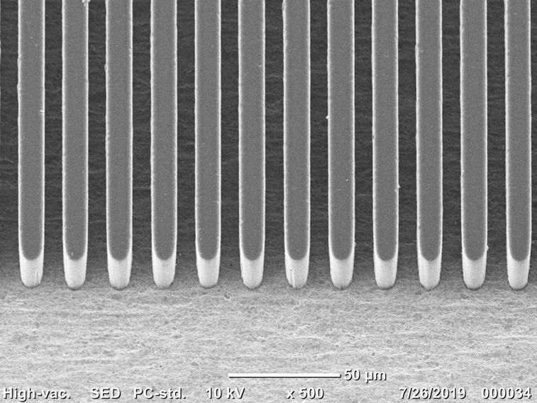
(b) Patterning demonstrated with 10 µm/10 µm L/S.
The photoresist is compatible with various tools, including either 405 nm or dual-band exposure, and works well at high photospeed to enhance productivity. Like DuPont’s other LDI photoresists, DI5100 deposition is a clean process with very low foaming and sludge formation, which avoids exposure to hazardous cleaning chemicals and reduces cost.
By introducing photoresists and other materials that have been proven to perform well when design rules push the limits of HDI PCBs, manufacturers will be better prepared to produce reliable SLP designs that meet the needs of tomorrow’s electronic devices.
Related Information
DuPont brings a deep understanding of high-performing materials to enhance printed circuit board materials reliability for flexible and rigid boards.

DuPont circuit imaging materials are specifically engineered to achieve higher yields with the most challenging circuit designs.

Ultra fast photospeed, high performance, and compatibility with conventional printed wiring board (PWB) processes are critical to help PWB fabricators optimize their LDI equipment investments.
We’re here to help.
We love to talk about how our electronics solutions can build business, commercialize products,
and solve the challenges of our time.