Fast, high-purity Cu plating enables next-gen devices
April 20, 2016
Copper plating has been a mainstay in advanced semiconductor packaging as the solution for forming the redistribution layers (RDLs), which are the conductive traces handling data coming in and out of the package as well as serving as a transition between small-scale I/Os of the chip and the much larger scale connections with the circuit board. Increasingly, copper has also been called upon as the solution to increasing I/O counts using pillars that can be formed in smaller scale and more densely than possible with traditional controlled collapse chip connection (C4) bumps. These high-density solutions are critical to improving the performance and reliability of high-performance 3DIC processor packages like those used in cloud servers. It’s clear, however, that 3DIC packaging won’t be the solution to driving improvements for all packaging applications.
Fan-out wafer-level packaging (FOWLP) technology allows increasingly dense area arrays in increasingly smaller silicon ICs to be cost-effectively connected to printed circuit boards. It's not a new approach, but after a decade of niche applications, it's now headed for much broader adoption. FOWLP can be designed in various ways to meet the needs of the global electronics device industry—including single-chip, multi-chip in a single-layer, and multi-chip multi-layer variations—and promises to provide an ideal balance of price:performance for high-volume consumer mobile applications.
To meet the price targets for consumer devices, the FOWLP process must be engineered to be extremely high throughput and relatively low-cost while meeting extraordinarily stringent performance specifications. In particular, the copper plating process used to form the redistribution layer (RDL) must be capable of forming precise line and space patterns as small as a single micron in width at a high plating speed. Ideally, the same copper plating chemistry in the same bath can be used to plate RDL as well as Cu pillars.
At the recent IMAPS Device Packaging conference, Dow presented solutions the company has been providing and is developing to address these market drivers. Dow’s Intervia™ 8540 Cu plating bath has been widely used for RDL plating and is a useful benchmark for new plating chemistries. During internal tests on 300 mm wafers, both Intervia™ 8540 and new 9000 chemistries perform exceptionally well at RDL plating, with low within-die height uniformity (WID), with nearly identical performance at equivalent plating rates. Intervia 9000 Cu does plate slightly less-domed profiles.

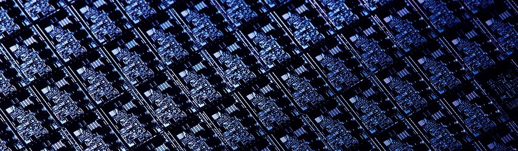
Figure 1: Copper-plating process used for the redistribution layer (RDL)
For Cu pillar applications, results for both Intervia 8540 and 9000 copper chemistries demonstrated strong performance. Plating baths for Cu pillars need to deposit pillars with flat tops and with high pillar height uniformity while maintaining high plating rates needed for fast wafer through-put. As such, the newer Intervia 9000 Cu chemistry is capable of plating pillars with flatter tops and at least 18 ASD (4 μm/min).
Prototype chemistries have also been developed and evaluated for plating megapillars typically used for fan-out applications. Cu pillars 50 microns in diameter plated with an early prototype chemistry demonstrated the ability to plate with flat tops at deposition rates of at least 20 ASD (4.4μm/min) without defects and with excellent WID performance. Another prototype chemistry also for fan-out applications demonstrated the capability of plating 200μm diameter Cu pillars as high as 40 ASD (8.8μm/min) with flat profiles and good WID performance.
To learn how Dow Electronic Solutions is optimizing its advanced electronics packaging materials for 3DIC and FOWLP, view this “Evaluation of Cu Pillar Chemistries” presentation from the 2016 IMAPS International Device Packaging Conference.
Related Information
DuPont understands the market needs and has developed a broad portfolio of semiconductor packaging materials for a range of technology areas.
DuPont Electronics & Imaging Materials’ copper pillar plating products meet the strict requirements for today’s most advanced applications.
We’re here to help.
We love to talk about how our electronics solutions can build business, commercialize products,
and solve the challenges of our time.