Lithographic Material Evolution Continues to Enable the Semiconductor Industry
Cheng-Bai Xu
Ph.D., Global R&D Director, Litho Technologies
December 18, 2019
Since the advent of the semiconductor era, sophisticated patterning materials have continually evolved to enable ongoing node reduction. Examples include custom-designed photoresist material developed using novel polymer and organic chemistry, as well as materials that address such critical issues as antireflection control, leaching and outgassing, defects, and pattern transfer. As the IC fabrication process has progressed, the industry has continued to adapt to new challenges that have arisen. Along the way, DuPont has taken a leading role in devising innovative solutions that have helped enable chipmakers to stay on the path of Moore’s Law (see Figure 1).
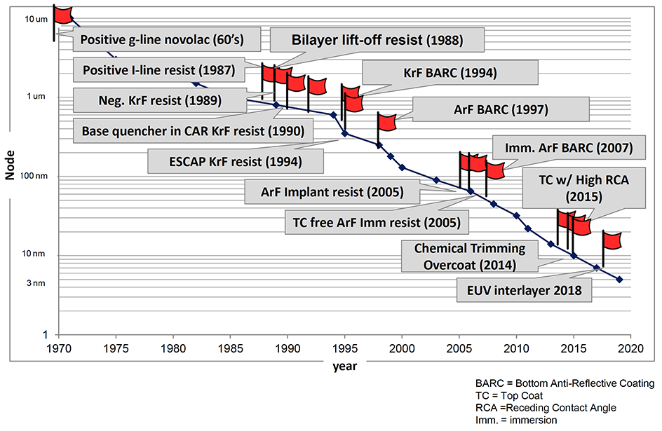
Figure 1. DuPont has consistently developed breakthrough material innovations at each major node.
Challenges for advanced chip manufacturing
As lithographic patterning extends to sub-10 nm nodes, chipmaking requires more complex lithography techniques in order to achieve optimal resolution and yield. Today, advanced circuit manufacturing faces three key challenges, each of which creates corresponding issues for lithography:
- Scaling down of critical dimensions (CD)
- Growing prevalence of 3D structures
- Escalating costs
Let’s take a closer look at each of these problems, their evolutionary paths, and some of the material solutions DuPont offers today to address them. (Note that, for each challenge, material solutions have been devised at both the resist level and at the functional layer, i.e. below and above the resist.)
CD Scaling
Photoresist chemistry is largely a function of wavelength. The challenge of tuning resists for wavelength reduction has driven lithography scaling for 50 years. When scaling demands moved the needle down to 248nm in the late 1980s, faster, more transparent resists were needed. Copolymers based on p- hydroxystyrene and t-butyl acrylate were especially successful, and became the standard-bearers for high-volume IC production.
Ten years later, the industry again scaled down, to the 193nm wavelength, requiring resist chemists to start once more from scratch to meet new transparency and etch-resistance constraints. Once the proper resin systems were identified, chemical amplification was applied to meet throughput requirements, and 193nm resists continued to evolve as imaging transitioned from dry to immersion lithography. Extending 193nm immersion lithography has allowed patterning far below the exposing wavelength.
Today, several problems prevail with respect to CD scaling:
- Poor resist resolution
- Poor linewidth roughness (LWR)/CD uniformity (CDU) of resist
- Resist pattern collapse
- Substrate damage caused by conventional wet etching process
At the resist level, materials are needed that offer compatibility with shorter wavelengths, high resolution, good LWR and profile, and a wide process window. DuPont has developed solutions that tackle these requirements. One example is enabling LWR/CDU improvements by optimizing resists, as shown in Figure 2.

Figure 2. DuPont delivers state-of-the-art resolution and LWR for 193nm resist using immersion lithography.
Functional layer (below and above resist) material solutions include:
- BARC, EUV interlayer (IL), and spin-on carbon (SOC), which deliver low reflectivity, minimal scum and pattern collapse, and high etch selectivity (etch trimming enables small CD). BARC and SOC both provide good gap filling and planarization properties. Additionally, DuPont’s SOC offers unique characterstic of being curable in both air and inert gas, such as nitrogen.
- Overcoat, which enables CD shrink after the lithography process. DuPont’s Chemical Trim Overcoat (CTOTM) is a photoresist trimming solution used to form finer photoresist patterns than that with direct imaging alone, and it doesn’t require additional photolithography steps. A CTO process (Figure 3) typically involves coating a CTO over a photoresist pattern, heating the wafer so that acid diffuses into the pattern and causes deprotection in a resist surface region, and developing the pattern to remove the surface region, thereby achieving smaller CD.
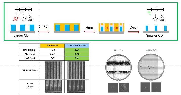
Figure 3. The CTO process developed by DuPont enables resist-line CD shrink, as shown at the bottom of the figure.
3D Topography
As design rules have shrunk in proportion to device scaling, implant lithography has become increasingly challenging. In addition to the ongoing lithographic challenges of traditional scaling, the industry has migrated from 2D planar gate structures to 3D FinFET designs. Similar NAND devices have adopted 3D structures, and multiple patterning processes involve complicated 3D topographies. The increased topography associated with 3D structures has proven highly challenging for patterning. To address the challenges associated with 3D structures, novel BARC and SOC materials are needed that offer high etch resistance, selectivity and planarization, and, in particular, the ability to fill gaps caused by 3D topography without creating voids. DuPont’s suite of application-specific BARC and SOCs fill these requirements to help the industry negotiate patterning challenges associated with scaling and 3D structures (see Figure 4).

Figure 4. DuPont’s advanced BARCs can fill gaps in 3D structures of 10nm and below with no voids.
At the resist level, DuPont solutions that are helping chipmakers cope with 3D topography challenges include:
- 248nm negative-tone resist with minimum scum (residual resist left on the developed area)
- Thick 248nm resist for 3D NAND
- 193nm resist with good CDU/LWR/profile and wide process window for 3D NAND
High Costs
With each new semiconductor innovation, there are attendant cost issues. Complicated multi-patterning processes are hampered by slow throughput and low yields, and are subject to a high number of defects. All of these factors add up to slower time to market and greater expense for the device maker. As touched on earlier, high-resolution resists are essential to helping resolve challenges associated with increasingly prevalent 3D structures and CD scaling. Fast photospeed is also needed, especially for EUV resists. DuPont has innovated a top coat-free resist with an embedded barrier layer (EBL) that offers a high receding contact angle to reduce immersion defects at high scan while mitigating leaching and defects instead of using an additional chemical of top coat. The EBL technology has created a fast throughput with low defects and cost, and a more environmentally-substainable process with less chemical consumption for the semiconductor industry.
Material solutions at the functional layer include high-contact-angle, low-defect top coats, and innovative BARC/SOC coatings as mentioned earlier. The illustration in Figure 5 contrasts a conventional BARC solution with DuPont’s ultra-thin BARC, which is a conformal coating. The thin BARC is used to reduce reflectivity; at a film thickness of < 15nm, it is sufficiently thin that device manufacturers can implant the source and drain regions directly through the thin BARC. This approach is attractive as it removes the BARC open-etch step, which can potentially damage today’s sensitive multilayer stacks. This reduces process complexity, thereby greatly helping to reduce costs.
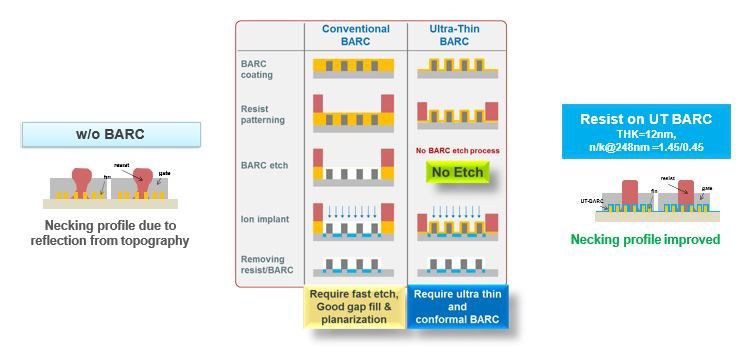
Figure 5. DuPont’s ultrathin BARC enables a low-cost implant process for complex topographies.
As this overview has illustrated, DuPont is well established as an industry leader in electronic and lithographic materials. Innovations like BARC have solved critical issues such as CD control, planarization and etch selectivity, and are addressing the challenges associated with complex device structures while helping to keep material costs in check. Novel materials will continue to play a critical role in advanced patterning, and DuPont will be at the forefront of future innovations.
Related Information
DuPont develops and delivers market-leading lithography materials to support semiconductor advanced patterning.
DuPont offers a production-proven line of ancillary lithography products to support a total patterning solution.
DuPont offers robust, production-proven photoresists for lithography that meet the requirements of generations of semiconductor processes.
We’re here to help.
We love to talk about how our electronics solutions can build business, commercialize products,
and solve the challenges of our time.