Fine-tuning CMP slurries for 3D TSV processes
Michelle Ho, Ph.D.
Slurry R&D Scientist, CMP Technologies, DuPont Electronics & Industrial
June 27, 2017
In semiconductor manufacturing, 3D stacking refers to technologies where chips are thinned, stacked and interconnected to each other or to a silicon interposer (TSI) using through silicon vias (TSVs). 3D stacking shrinks the overall device form factor, enhances performance, reduces power consumption and increases reliability. While these advantages have been well understood for some time, the cost factor of TSV processes has limited TSV adoption to memory in high-performance computing applications, image sensors and MEMS applications. Over the past year, after a long journey from R&D to manufacturing, TSV technologies have finally made it to the mainstream. As the semiconductor industry shifts its roadmap focus from Moore’s law to heterogeneous integration through advanced packaging applications, it is expected that TSVs will continue to play a significant role in advanced 3D integration processes.

Figure 1: 3D Stacking Design
Chemical Mechanical Planarization in TSV Processes
Chemical mechanical planarization (CMP) is used at multiple process steps in TSV and is one of the most critical elements in the process flow. CMP is used to attain excellent wafer topography. The results of the process must avoid corrosion, minimize dishing, minimize surface roughness, enable clear electroplating and help ensure predictable, controlled consistent film isolation. The "chemical" part of CMP involves a CMP slurry materials platform comprised of oxidants, abrasives, pH adjuster, surface protector, removal rate tuner and defect reduce.

Figure 2: CMP Slurry Interaction
Currently, there are three process flows used for fabricating and metallizing TSVs. They are defined as via first, via middle and via last. Via first is a front-end process performed before device fabrication. Via middle takes place after device fabrication, before metal traces are formed. Via last is a back-end process that takes place after metallization, and that can be handled by either the fab or an outsourced semiconductor assembly and test (OSAT) facility.
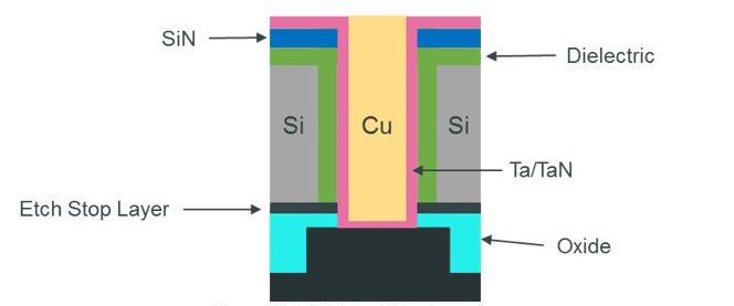
Figure 3: TSV Film Structure
Regardless of which approach is used, there are four distinct process steps during which CMP is required to create a robust TSV film structure: after Cu-fill, TSV barrier, via reveal and post oxide deposition prior to permanent bonding. When these steps are performed is based on whether a via first, via middle or via last approach is being used. Each step benefits from a CMP slurry that is tunable such that it can meet the varied topography requirements. Of all the slurry elements involved, the two most important to consider for optimal TSV films are the abrasive used for removing soft layers, and the removal rate tuner for controlling film isolation.
Fumed Silica vs. Colloidal Silica Abrasives
There are two types of abrasives used in CMP slurry today: fumed silica and colloidal silica. Each has its advantages and disadvantages.
Fumed silica is a pyrogenically formed powder via a gas phase reaction. Forced in liquid suspension, it exhibits high purity and an irregular structure. With fumed silica, there is concern about porosity control. Additionally, it is prone to agglomeration, particularly if it is pH-shocked, so dilution must be performed carefully. While fumed silica is hard to control on the wafer surface, it can achieve a faster removal rate with higher abrasion because of the size and shape of its particles.
Colloidal silica, on the other hand, is formed in a liquid phase, which is a more controllable chemical reaction. It therefore consistently exhibits nonporous, independent, spherical particles. Its strong alkaline composition means it is stable in a wide variety of chemistries, including potassium hydroxide and ammonium hydroxide, as well as a proprietary acid tested at DuPont. It has a relatively higher trace metal content than fused silica, but can be lowered by ion exchange. While results are more controllable than with fumed silica, the removal rate is slower, which can extend the time it takes to perform the CMP step.

Figure 4: (a) Fumed Silica and (b) Colloidal Silica (c) Elongated Colloidal Silica
DuPont Slurry Solutions for TSI and TSV
Recognizing the advantages of fumed and colloidal silica, DuPont Electronics & Industrial, in partnership with EMD Performance Materials, has engineered a new particle based on colloidal silica that exhibits the benefits of both. Synthesized by adjusting the manufacturing conditions of conventional spherical particles, the resulting elongated particle exhibits good planarization, a higher removal rate than either fumed or colloidal silica, and good dilution capabilities. When applied to a slurry, this elongated particle facilitates a higher removal rate than both fumed and colloidal silicas.
The removal rate tuner is the other slurry element that can have a significant impact on its performance. The performance of the tuner is dependent upon the additives used. Some additives randomly absorb on the substrate, while others self-assemble. Those that randomly absorb result in non-targeted films with moderate steric inhibition. The capability to reduce contact stress is limited. However, lower protection results in a higher removal rate.
Tuners that self-assemble result in targeted films with strong steric inhibition. They have a stronger ability to reduce contact stress, but strong protection reduces the removal rate. Factors influencing the absorbate formation structure on the substrate include electrostatic force, hydrophobicity, concentration and mechanical force in contact.
By selecting suitable additives and the most favorable concentration, slurries can offer tunable selectivity for different films and therefore meet the requirements of various TSV devices to provide good global uniformity after polish. DuPont Electronics & Industrial has been working to develop performing additive technologies that achieve better stability, low defectivity and tunable selectivity.
Combined, DuPont elongated silica and removal rate tuners have resulted in production-proven CMP slurry platforms. DuPont portfolio includes solutions developed for various film stacks for front-side TSV and interposer integration, including the Acuplane™ 4100 and Acuplane™ 2010 slurry series; as well as backside TSV integration, such as BSP120; with additional solutions in development. These technologies have been successfully adopted for a variety of applications and the platforms are fully tunable to customers’ specific device needs.
If you’d like to learn more about electroplating for 3D TSVs, DuPont has a tutorial series on this topic. See Part 1: The Fundamentals of Copper Electroplating and Part 2: Plating Challenges of TSVs .
Related Information
DuPont understands the market needs and has developed a broad portfolio of semiconductor packaging materials for a range of technology areas.
Discover DuPont’s range of materials offerings for CMP, including slurries and hard/soft polishing pads for many CMP applications.
We’re here to help.
We love to talk about how our electronics solutions can build business, commercialize products,
and solve the challenges of our time.